Manufacturing Capacity Expansion
Amber Group Conducts Ground Breaking Ceremony for Two Advanced Manufacturing Facilities at YIEDA, Jewar
NSE
amber
BSE
540902
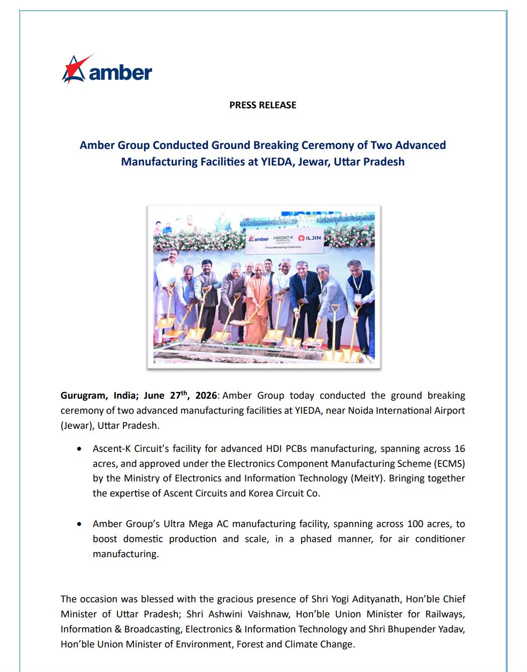
Amber Enterprises India Limited has conducted the ground breaking ceremony for two advanced manufacturing facilities at the Yamuna Expressway Industrial Development Authority (YIEDA), Jewar, Uttar Pradesh. The projects include a 16-acre HDI PCB manufacturing facility under Ascent-K Circuits and a 100-acre Ultra Mega AC manufacturing facility, reinforcing the company’s domestic manufacturing capabilities and supporting India’s electronics manufacturing ecosystem.
PRICE-SENSITIVE TRIGGER
Event: Ground breaking ceremony for two advanced manufacturing facilities at YIEDA, Jewar, Uttar Pradesh.
Type: Manufacturing Capacity Expansion
Impact: Positive
Immediate Effect: The projects strengthen Amber Group’s long-term manufacturing footprint in electronics components and air conditioner production while supporting domestic value addition, import substitution and future production capacity expansion.
Key Metrics:
- HDI PCB Manufacturing Facility: 16 Acres
- Ultra Mega AC Manufacturing Facility: 100 Acres
- Government Scheme: Electronics Component Manufacturing Scheme (ECMS)
- HDI PCB Technology Partner: Korea Circuit Co.
Highlight:
- Amber Group commenced development of two strategic manufacturing facilities spanning 116 acres, targeting advanced PCB manufacturing and large-scale air conditioner production in Uttar Pradesh.
What Happened ?
Amber Enterprises India Limited announced the successful ground breaking ceremony for two advanced manufacturing facilities at YIEDA, near Noida International Airport (Jewar), Uttar Pradesh.
The expansion comprises a 16-acre High Density Interconnect (HDI) Printed Circuit Board (PCB) manufacturing facility under Ascent-K Circuits and a 100-acre Ultra Mega Air Conditioner manufacturing facility. The PCB project has been approved under the Electronics Component Manufacturing Scheme (ECMS) of the Ministry of Electronics and Information Technology (MeitY) and combines the technological expertise of Ascent Circuits and Korea Circuit Co.
The ceremony was attended by senior central and state government leaders, highlighting the strategic importance of the investment in India’s electronics manufacturing ecosystem.
Key Details
Manufacturing Expansion:
- Ground breaking ceremony conducted at YIEDA, Jewar, Uttar Pradesh.
- Development of two advanced manufacturing facilities.
- Expansion supports Amber Group’s long-term manufacturing strategy.
HDI PCB Manufacturing Facility:
- Facility spread across 16 acres.
- Dedicated to manufacturing advanced High Density Interconnect (HDI) Printed Circuit Boards.
- Approved under the Electronics Component Manufacturing Scheme (ECMS).
- Collaboration combines the expertise of Ascent Circuits and Korea Circuit Co.
- Intended to strengthen domestic electronics component manufacturing and reduce import dependence.
Ultra Mega AC Manufacturing Facility:
- Manufacturing campus spanning 100 acres.
- Designed for phased expansion of air conditioner manufacturing capacity.
- Expected to enhance domestic production scale and manufacturing efficiency.
Strategic Significance:
- Supports India’s Atmanirbhar Bharat initiative.
- Enhances domestic value addition in electronics manufacturing.
- Promotes innovation in PCB manufacturing technology.
- Expected to generate employment opportunities in Uttar Pradesh.
- Strengthens Amber Group’s manufacturing ecosystem across electronics and consumer durables.
Note:
- Management stated that the expansion represents a strategic investment in technology-intensive manufacturing capabilities and is expected to improve India’s self-reliance in electronics manufacturing over the long term.
Risk Analysis
Summary:
- The projects represent long-term capacity expansion initiatives. Their commercial success will depend on timely execution, commissioning, demand growth and successful scaling of manufacturing operations.
Key Risks:
- Project execution and commissioning delays.
- Capital expenditure recovery depends on future capacity utilization.
- Demand fluctuations in the consumer durables and electronics sectors.
- Technology implementation and operational ramp-up risks for the HDI PCB facility.
Worst Case:
- Delays in construction, slower capacity utilization or weaker market demand could postpone revenue generation and reduce expected returns from the investment.
Risk Level: Medium
Company Commentary
- The expansion marks a significant milestone in Amber Group’s strategy to build large-scale technology-intensive manufacturing capabilities.
- The projects support the vision of Atmanirbhar Bharat through increased domestic manufacturing.
- The HDI PCB facility is expected to deepen domestic value addition and foster innovation in India’s electronics ecosystem.
- The investment is expected to create employment opportunities in Uttar Pradesh.
- Management believes the facilities will strengthen India’s manufacturing competitiveness in electronics components and air conditioning products.
Official Exchange Filing: Amber Enterprises India Limited